Investigation of Graphene-Based Nanomaterials for Advanced Electronic Applications
DOI:
https://doi.org/10.65521/apl.v9i1.4283Keywords:
Abstract
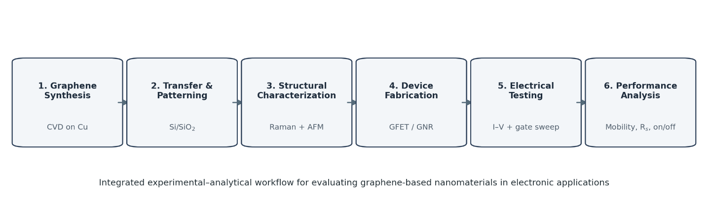
Graphene-based nanomaterials combine atomic-scale thickness with high carrier mobility, tunable electrostatic response, mechanical flexibility, optical transparency, and large current-carrying capability, making them attractive for high-frequency transistors, transparent electrodes, sensors, and other emerging electronic systems. This methodology paper establishes a reproducible framework for investigating how synthesis quality, structural defects, dimensional confinement, and device geometry influence electronic performance. The proposed workflow integrates chemical vapor deposition (CVD) growth on copper, polymer-assisted transfer to Si/SiO2 substrates, Raman and atomic-force-microscopy characterization, lithographic formation of graphene field-effect transistor (GFET) or nanoribbon channels, and current-voltage/gate-voltage measurements. Primary response variables are sheet resistance, charge-neutrality voltage, field-effect mobility, current on/off ratio, and, for confined structures, effective transport gap. A literature-bounded demonstration dataset is used only to show how the analytical pipeline operates; it is not presented as newly measured experimental data. The framework is designed to distinguish conductivity-oriented applications, where pristine large-area graphene is preferred, from switching applications, where controlled band-gap opening through nanostructuring or bilayer electrostatics is required. The study concludes that graphene is especially compelling for radio-frequency, transparent, sensing, and interconnect functions, while its zero-band gap remains a central limitation for conventional digital logic.