Optical and Electrical Properties of Graphene-Based Nanostructures
DOI:
https://doi.org/10.65521/apl.v10i1.4453Keywords:
Abstract
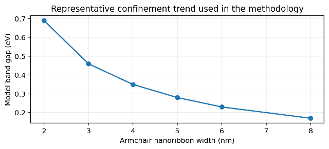
Graphene-based nanostructures combine the exceptional carrier transport of two-dimensional graphene with size-, edge-, and doping-dependent electronic and optical responses. This methodology paper develops a compact computational framework for studying pristine graphene, graphene nanoribbons, and graphene quantum dots using a nearest-neighbor tight-binding description, Kubo-type optical conductivity, and Landauer electrical transport. The procedure defines atomistic geometries, calculates energy bands and density of states, evaluates optical transition spectra, and estimates conductance while systematically varying ribbon width, edge configuration, quantum-dot size, and Fermi-level position. Validation is anchored to well-established observations including the approximately 2.3% visible-light absorbance of monolayer graphene, width-dependent band-gap opening in nanoribbons, and tunable optical transitions in confined graphene structures [2-4,9-14]. Representative model results show that lateral confinement opens a band gap in armchair nanoribbons, shifts the first optical transition to higher energy as dimensions decrease, and suppresses low-bias conductance near charge neutrality. Electrostatic doping, in contrast, preserves the zero-gap character of extended graphene while changing intraband conductivity and suppressing low-energy interband transitions through Pauli blocking. The proposed methodology is suitable for comparative design studies of graphene optoelectronic structures before more expensive density-functional or many-body calculations are performed.