Analysis of Semiconductor Thin Films for Solar Cell Applications
DOI:
https://doi.org/10.65521/apl.v5i1.4241Keywords:
Abstract
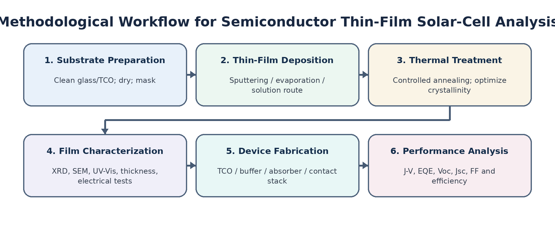
Semiconductor thin films are central to second-generation and emerging photovoltaic technologies because they combine strong optical absorption with reduced material consumption and compatibility with large-area processing. This methodology paper presents a reproducible framework for analyzing thin films intended for solar-cell absorbers and functional layers. The approach integrates controlled film deposition and annealing with structural, morphological, optical, electrical and device-level characterization. X-ray diffraction is used to identify crystalline phases and estimate crystallite size; scanning electron microscopy is used to evaluate grain morphology and surface continuity; UV-visible spectroscopy is used to determine transmittance, absorption coefficient and optical band gap; and four-point-probe or Hall measurements are used to quantify sheet resistance, resistivity, carrier density and mobility. Selected films are incorporated into a photovoltaic stack and evaluated under AM1.5G illumination using current-density-voltage and, where available, external quantum-efficiency measurements. The literature available up to 2016 demonstrates that CIGS and CdTe thin-film cells had surpassed 22% laboratory efficiency, while perovskite cells had reached a comparable level and CZTSSe remained lower but attractive because of earth-abundant constituents. The proposed workflow therefore emphasizes correlations among microstructure, optical absorption, electrical transport and photovoltaic parameters rather than relying on any single characterization result. The framework is suitable for systematic comparison of semiconductor thin films and for identifying processing conditions that maximize solar-cell suitability.