Investigation of Optical and Electrical Properties of Thin Film Semiconductor Materials
DOI:
https://doi.org/10.65521/apl.v7i1.4268Keywords:
Abstract
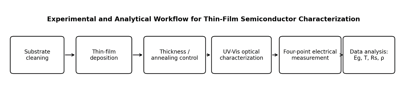
Thin-film semiconductors are central to photovoltaic cells, transparent electronics, photodetectors, displays, and sensor platforms because their optical absorption, band-gap energy, charge transport, and electrical resistivity can be tuned through material choice, thickness, deposition conditions, doping, and post-deposition treatment. This methodology paper presents a compact experimental framework for investigating the coupled optical and electrical properties of representative thin-film semiconductor materials, with zinc oxide (ZnO), cadmium sulfide (CdS), and cadmium telluride (CdTe) used as model systems. The proposed workflow integrates controlled deposition, thickness verification, UV-Visible spectrophotometry, optical-band-gap estimation through the Tauc approach, refractive-index/thickness analysis through the Swanepoel method where interference fringes are available, and four-point-probe measurement of sheet resistance and resistivity. X-ray diffraction and surface microscopy are included as supporting checks because structural disorder and grain development can influence both photon absorption and carrier transport. The literature review is restricted to work published in 2018 or earlier. The expected outcome is a reproducible relationship among film thickness, visible transmittance, absorption edge, optical band gap, sheet resistance, and resistivity. The framework is suitable for comparative screening of thin-film materials before device fabrication and emphasizes transparent reporting of measurement conditions and uncertainty.