Optical And Electrical Properties Of Semiconductor Thin Films For Photovoltaic Devices
DOI:
https://doi.org/10.65521/apl.v9i1.4279Keywords:
Abstract
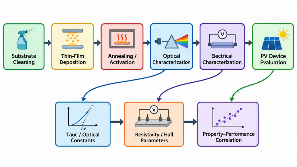
Semiconductor thin films are central to photovoltaic (PV) technologies because they enable strong light absorption, reduced material consumption, tunable electronic structure, and scalable device fabrication. This methodology paper presents an integrated experimental framework for evaluating the optical and electrical properties of photovoltaic thin films, with particular relevance to CdTe, Cu(In,Ga)Se2 (CIGS), Cu2ZnSnS4 (CZTS), amorphous silicon, and emerging halide-perovskite absorbers. The proposed workflow combines controlled deposition and annealing with UV–visible spectrophotometry, Tauc analysis, thickness/refractive-index analysis, X-ray diffraction, surface morphology measurements, four-point-probe resistivity, Hall-effect measurements, and current density–voltage characterization. The central objective is to connect film quality—absorption coefficient, band gap, resistivity, carrier density and mobility—to photovoltaic figures of merit. A representative optimization dataset is included to demonstrate how annealing-dependent changes can be interpreted without presenting the values as experimentally measured results. The methodology emphasizes repeatability, calibration, statistical replication, and physically consistent cross-checking of optical and electrical data. Literature published up to and including 2020 is used. The framework can be applied to different semiconductor absorbers and buffer/contact layers and is suitable for laboratory-scale screening before full device optimization.