Investigation of Quantum Tunnelling Effects in Nanoscale Semiconductor Devices
DOI:
https://doi.org/10.65521/apl.v10i1.4443Keywords:
Abstract
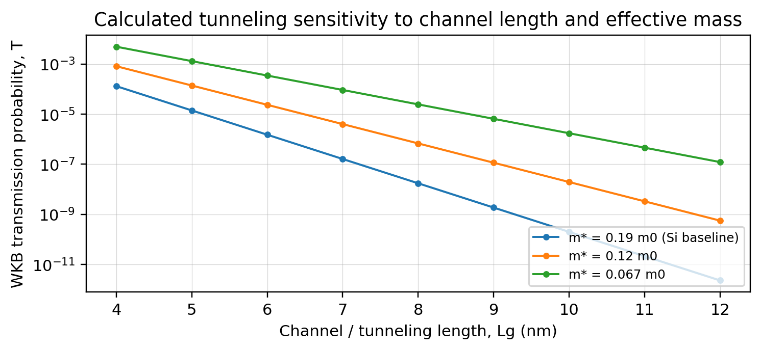
As semiconductor dimensions approach the sub-10-nm regime, the wave nature of carriers becomes a primary determinant of device behavior. This paper investigates direct quantum tunneling in nanoscale semiconductor devices using a methodology that combines the Wentzel-Kramers-Brillouin (WKB) approximation for rapid tunneling estimates with the Landauer and nonequilibrium Green's function (NEGF) formalisms as the transport framework. A double-gate silicon MOSFET is used as the reference structure, and the dependence of source-to-drain tunneling on channel length, barrier height, and transport effective mass is examined. For a 0.25 eV off-state barrier and an electron transport mass of 0.19 m0, the calculated WKB transmission increases from 2.30 x 10^-12 at 12 nm to 1.32 x 10^-4 at 4 nm, corresponding to an increase of approximately 5.7 x 10^7 in the tunneling leakage index. Lower effective mass further increases transmission, demonstrating the trade-off between high carrier velocity and leakage control in aggressively scaled channels. The results support the use of quantum-transport-aware design, material selection, and electrostatic barrier engineering as essential strategies for nanoscale transistor development.