Analysis of Quantum Confinement Effects in Semiconductor Nanostructures for Optoelectronic Applications
DOI:
https://doi.org/10.65521/apl.v8i1.4275Keywords:
Abstract
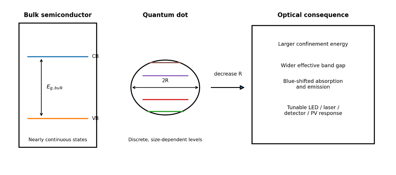
Quantum confinement provides a direct route for engineering the electronic and optical behavior of semiconductor nanostructures because carrier motion becomes spatially restricted when one or more dimensions approach the exciton Bohr radius. This methodology paper develops a reproducible theoretical framework for analyzing the size dependence of the effective band gap and the corresponding optical transition wavelength in semiconductor quantum dots, using CdSe as a representative material. The approach combines the effective-mass approximation with the Brus confinement expression, including electron and hole kinetic-energy terms and first-order electron-hole Coulomb attraction. A radius sweep from 2 to 6 nm is used to quantify the transition from strong toward weaker confinement. The computed results predict an optical gap increase from the 1.75 eV bulk value to approximately 2.54 eV at a 2 nm radius, corresponding to a wavelength shift from about 709 nm to 488 nm. The analysis therefore demonstrates the inverse relationship between nanostructure size and transition energy and connects this tunability to light-emitting diodes, lasers, photodetectors, electroabsorption devices and photovoltaic absorbers. The framework is intended as a transparent methodology rather than a replacement for atomistic calculations; surface states, finite barriers, dielectric mismatch and non-parabolic bands are identified as key extensions for device-specific modeling.